Analysis and Electrical Characterisation of Vertical Nanowire Trench Metal-Oxide-Semiconductor Barrier Schottky Rectifiers
Hey there! Are you curious to know what module 12 - the Bachelor thesis - entails? Keep on reading! My name is Maarten and I will tell you all about how I battled my way through the last eleven weeks of my Bachelor. If you do not yet know me, you can flip back to the start of this Vonk and read all about me and my fellow board members! I have worked on my thesis called “Analysis and Electrical Characterisation of Vertical Nanowire Trench Metal-Oxide-Semiconductor Barrier Schottky Rectifiers” at Integrated Devices and Systems (IDS). For obvious reasons I shall abbreviate the diode name to VNW-TMBS.
I started my assignment on the 23rd of April last academic year, but I was already looking around for a potential assignment in the last weeks of module 11, something that saves time in module 12 for the assignment itself. In those last weeks, I explored the possibilities and made appointments at research chairs of interest. Do not be afraid to just e-mail or walk by professors in your discipline of interest, an assignment does not present itself. For me it was rather straightforward: my programming skills have never been exceptionally tremendous, I have always been interested in physics and the mathematical and theoretical side of electrical engineering. After a couple of meetings and reading some interesting papers, I came to the decision to graduate at the research chair of IDS. However, I was not there yet, within IDS I still had a wide variety of assignments to choose from; ranging from micro-sensors up to transistor characterisation. After several talks with professors I decided to analyse and characterise the intriguing VNW-TMBS diodes.
The first few weeks of the Bachelor assignment are often the worst ones. The roster is completely empty, except for the weekly meetings with your supervisor(s); everything comes down to your own effort and motivation. I noticed that an overwhelming majority of my peer students had no clue where and how to start their research. Since I was doing research in the area of device physics, I guessed that the best way to start is to revise the Device Physics course of module 7a, large parts of the subject had subsided anyways. Afterwards I spoke to some Master students and asked for books of Master courses in the same discipline. During appointments with my supervisors we arranged the external members of my graduation committee and I received more papers and articles to read about all kinds of rectifiers and new concepts.
The VNW-TMBS diodes which I investigated are 3-Dimensional silicon Schottky diodes. The diodes discussed in modules 3 and 7a are all 1-Dimensional, this implies that the structure only varies in two dimensions. The rectifier I was dealing with has a complex nanostructure which varies in two dimensions, in order to adopt various physical effects which enhances the electrical performance. The fundamental trade-off in power rectifiers is that of the on-state resistance (forward) and the breakdown voltage (reverse), this also became the essence of my thesis. The Schottky part of the topic might (or should) sound more familiar, a Schottky contact implies that a semiconductor forms a junction with a metal. This structure can best be described by the energy band diagram of Figure 1.
![Figure 1:Energy band diagram of a Schottky contact with n-type semiconductor in thermal equilibrium[1]](figure%201.png)
Figure 1:Energy band diagram of a Schottky contact with n-type semiconductor in thermal equilibrium[1]
The energy band diagram of this Schottky diode is basically the energy landscape (vertical axis) plotted against distance or depth through the device (horizontal axis), and the Fermi level is indicated accordingly. Due to the negative doping in the semiconductor, a built-in voltage arises with an energy equal to q (elementary charge) times the voltage. The junction causes a region of space charge denoted by W0. However, the most interesting property of Schottky junctions is the Schottky barrier height, caused by the built-in voltage and abbreviated by ΦBN. Due to the Schottky barrier, the primary mechanism of conduction is the thermionic emission current (Jns), which strongly depends on this barrier height. The current in forward mode can be described as the following, where A*n is Richardson constant [2].
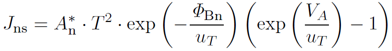
Formula 1
A low Schottky barrier allows for more current to flow in forward mode. When looking at the reverse mode, and assuming a bias voltage much larger than the thermal voltage, the leakage current can be described as [2]:
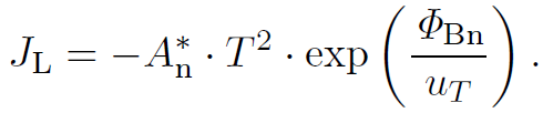
Formula 2
In order to minimise the leakage (or in fact increase the rectification), a large barrier height is favoured, this contrast reflects the fundamental trade-off in rectifiers. By experimenting with different types of nanostructures, varying numerous physical parameters, and looking into various physical effects, the trade-off can be improved.
Since the objective of my assignment was to analyse and characterise the VNW-TMBS diodes, eventually I had to perform series of measurements. In order to get acquainted with the measurement setup and equipment, I received trainings in the third week. Finally, the fun and exciting part could start. The background research has been done and the first sections of the report were written, it was time to gather as much data as possible! Figure 2 shows the complete measurement setup.
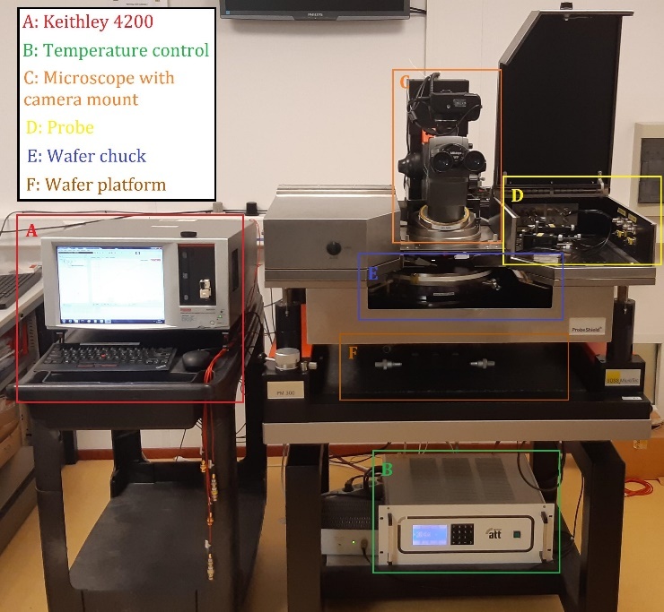
Figure 2: Labelled overview of the complete measurement setup, the Keithley 4200(left) connected to the PM 300 probe station(right).
Fortunately, I was able to schedule all the measurement timeslots myself. This gave a lot (convenient) flexibility, for some reasons I never reserved the measurement setup on Friday (mornings). Nevertheless, I have spent lots of days and afternoons in the Measurement Test Centre in Carré.
In the last few weeks the focus shifts to the report, I handed-in multiple preliminary and concept versions and received useful feedback from different people. Eventually ‘D-day’ came closer and closer: the presentation of the thesis. If you think that presenting is nerve-wracking, the questions that are fired at you afterwards are even worse. Fortunately, this went quite well and soon we could all enjoy the free drinks in the sun, discussing end results with peers and supervisors. At last, I really enjoyed my assignment, a good balance between in-depth theoretical research and hands-on measuring.
Bibliography
[1] B.J. Baliga. Fundamentals of Power Semiconductor Devices. Springer, New York, 2008. pp. 167 - 199.
[2] R.J.E. Hueting. Semiconductor Devices Explained More. University of Twente, October 2013. Department of Electrical Engineering, Mathematics and Computer Science.