Modelling and characterisation of a pressure sensor implemented in surface channel technology
One of the easiest pressure sensors to design is a resistive pressure sensor. A structure under pressure changes in geometry which causes the resistance of the structure to change. This change in resistance can be measured with an electronic readout circuit. But, how does this sensor precisely work? In my bachelor assignment I made a theoretical model of the working principal of a resistive pressure sensor.
It all starts with taking a trip into the domain of a mechanical engineer. The starting point is the geometry of the structure and the way this structure behaves under pressure. For my bachelor assignment, I used the assumption that the structure was a rectangular beam, fixed by a substrate at both ends. This assumption resulted in a formula which describes the deflection for this kind of structure.
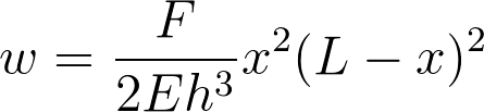
Formula 1
The formula is based on the dimensions of the structure and the Young’s Modulus of the material of the sensor. In the case of my bachelor assignment, the material of the sensor is gold and the material of the structure underneath is SiRN (Silicon Rich Silicon Nitride). Gold has a Young’s Modulus of approximately 80 GPa, SiRN has a Young’s Modulus of approximately 210 GPa. When the structure is subjected to pressure, the SiRN will determine the movement, because it is the stiffer material. Because of this, for determining the deflection, the Young’s Modulus of SiRN is used and it can be assumed that the gold sensor does not influence the movement of the SiRN structure. To give you a feeling about the difference in dimensions: the SiRN structure has a thickness of 3.5 µm and the gold has a thickness of 0.21 µm.
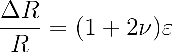
The formula for the deflection can be derived to find the strain at every point in the rectangular beam.
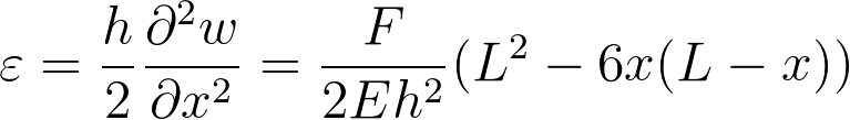
Formula 2
The strain is also known as the relative elongation of the structure. In simple words; a measure for how much longer the material became because of the pressure. In my bachelor assignment, rectangular beams were placed at 3 different positions along the width of a channel. Figure 1 shows the positions of the rectangular beams on top of a channel. The rectangular beams at the sides (R1 & R4) are compressed and the beams in the middle (R2 & R3) are elongated. The compressed beams have a negative strain and the elongated beams have a positive strain. The strain from the rectangular beams has a linear relation with the change in resistance, this is because the resistance of material is largely dependent on the length and area.
Formula 3
This linear relation is important for getting a formula for the electronic readout of the sensor. Before we get to this electronic readout, we first need to know how this rectangular beam becomes a pressure sensor.
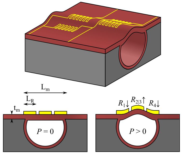
Figure 1: Design of a resistive pressure sensor. Gold strain gauges are placed on top of a channel roof. When under pressure the strain gauges are elongated and compressed changing their resistance.
In theory, a single rectangular beam, also known as a strain gauge, can be used as a pressure sensor. Most likely this will not give very accurate or reliable results. Therefore, multiple rectangular beams are combined in a meandering pattern to form a bigger strain gauge. Four of those bigger strain gauges are placed in a configuration that every Electrical engineering student knows; the Wheatstone bridge. Figure 2 shows all the resistors involved in the Wheatstone bridge. The strain gauges in a Wheatstone configuration make the results more reliable because four strain gauges are used to obtain a result. To give a short recap up until this point; a pressure sensor is made up from four strain gauges that are placed in a Wheatstone configuration. Each strain gauge is subjected to a positive or negative strain which results in a change in resistance.
Because of the linear relation between the strain and the resistance, the change in resistance of each of the Wheatstone resistors can be expressed as a strain.
Formula 4
Using this in the formula for a Wheatstone configuration leads to a formula for the output voltage of the total sensor.
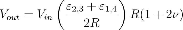
Formula 5
The problem with this formula is that parts connecting the pressure sensor to the power supply and measurement setup are neglected. Those parts do have a relevant length and lower the supplied voltage. To solve this, Vin needs to be compensated with the connecting parts.
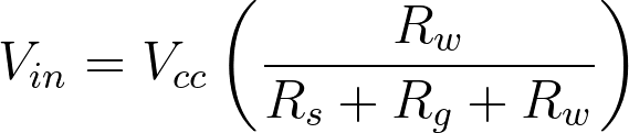
Formula 6
In this formula, Rs and Rg correspond to Figure 3. Rw is the resistance of the pressure sensor in rest position. The value of Rs and Rg is dependent on the design of the pressure sensor. The ideal situation would be to have the voltage supply and the readout circuit directly connected to the Wheatstone configuration. The contribution of Rs and Rg would be minimal. This would decrease the total resistance of the pressure sensor making it more sensitive. Realising this brings a lot of design issues, the connections of the power supply and readout circuit would have to be placed at difficult positions on the chip making it difficult to connect the chip with wires.
Combining all the separate formulas, a model is created that gives the sensor output as a function of the applied pressure. This sensor output can be used to look at the sensitivity of a pressure sensor. As already mentioned before, the sensitivity can be improved by making sure that all the connecting parts are as small as possible. In current applications, there is a trade-off between a higher sensitivity and a complex design which is necessary to reach this sensitivity. In my bachelor assignment, I used a theoretical model to validate results from several existing pressure sensors. The results from this showed that a lot of progress can be made in the accuracy of the fabrication process of the microchips.
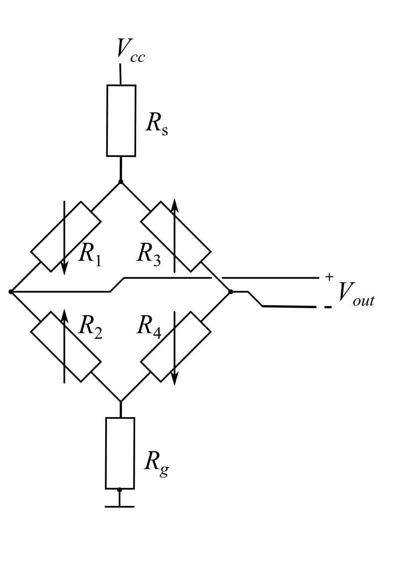
Figure 2: Circuit diagram representing the Wheatstone bridge.