Analyzing a Bottom-Switched Current Source Topology for Digital to Time Converters at Low Supply Voltages
In today’s world electronic devices are all around us. A primary building block within these devices is the Digital-to-Analog Converter (DAC). This block can convert a digital signal (i.e. a code consisting of 1’s and 0’s) into an analog signal by for instance switching on/off current sources using switches. A traditional switching method requires 2 overdrive voltages to make this work. If this voltage can be reduced, applications can work at lower supply voltages which saves power. A new switching technique is build and tested in a Digital-to-Time Converter (DTC) application.
DTC
Digital to Time converters can convert a digital input code to a certain time delay of a clock edge. It does this by discharging a capacitor C0 until the voltage across this capacitor crosses a threshold of a comparator which in turn detects a clock transition. Now, the key element of this DTC is to vary the moment this threshold voltage VTH is reached. [1] uses different start voltages on the capacitor to accomplish this. These different start voltages are created using a current switched DAC and a resistor. If the start voltage is set, the capacitor is discharged using a constant current and thus we create different threshold moments, see figure 1. In previous works, the discharging slope was changed by varying the current on this capacitor C0.
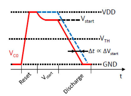
Figure 1: One cycle of voltage on capacitor C0.
Top and Bottom switching
Traditionally the current sources in the DAC are switched at the Top side. This is the left circuit in figure 2b. The current source and the switch can be implemented using transistors, which for the left case in 2b both have to be in saturation which requires 2 overdrive voltages. A new switching technique, where the current source is switched at the bottom of the current source, allows the switch to operate in the triode region, requiring a much lower voltage to operate. This means that the combination can run at a lower power which is more efficient. An example of a 5 bit DAC to create a start voltage can be seen in 2a, where 5 cells are chained together to create a variable Iout. In this article the two different Top and Bottom switching techniques are compared to see if the new bottom switched technique has a similar performance.
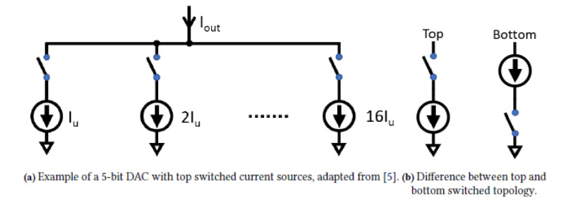
Figure 2: Illustration of 5-bit DAC and top/bottom switching.
Method
To find the performance, multiple tests were conducted. The two main experiments are elaborated here. The first one is testing the compression of the output current created by the DAC. What happens here is that with each increase in the digital code, an additional current cell is connected to the output and the output impedance of the DAC changes. This gives a nonlinear increase in the output current with respect to the increase in digital code. This can be seen in figure 3. Preferably, the amount the output current changes per digital code step should be the same for every step. But due to added impedance when connecting an additional current source, this is not the case. Both top and bottom switched topologies will suffer from this compression.
The second test concerns the switching speed of the DAC. Due to the position of the switch, the current source will have a different turn on behavior which has an influence on the DAC speed. Since this DAC determines the start voltage of the capacitor in the DTC, the results of these tests will reflect in the performance of the DTC. A new measurement technique is developed which determines the linearity of the average DAC output current over a certain time window. Here the linearity aspect is determined by looking at the average current over this time window for all codes and then taking an endpoint INL. The speed is determined by looking at this average linearity by decreasing this time window over which is averaged. This measurement was called the INLEA. With this new measurement technique it is not only possible to see how the INL is different between the Top and Bottom topologies, but also the difference between these two topologies over different time windows.
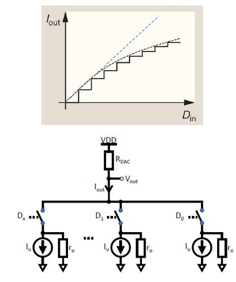
Figure 3: Top: Illustration of output current compression. Bottom: More cells connected to the output change the output seen at impedance.
Results
The results of these two experiments can be seen in figure 4. The compression of the output current is noticeable by the parabolic shape of the INL. This can be explained by looking at the top figure of figure 3. What happens during an endpoint INL is that a straight line is drawn between the endpoints of the measured data and that distance between this straight line and the other datapoints is the non-linearity. That is the reason for the parabolic shape as the measured data in the middle is most distant to the straight line.
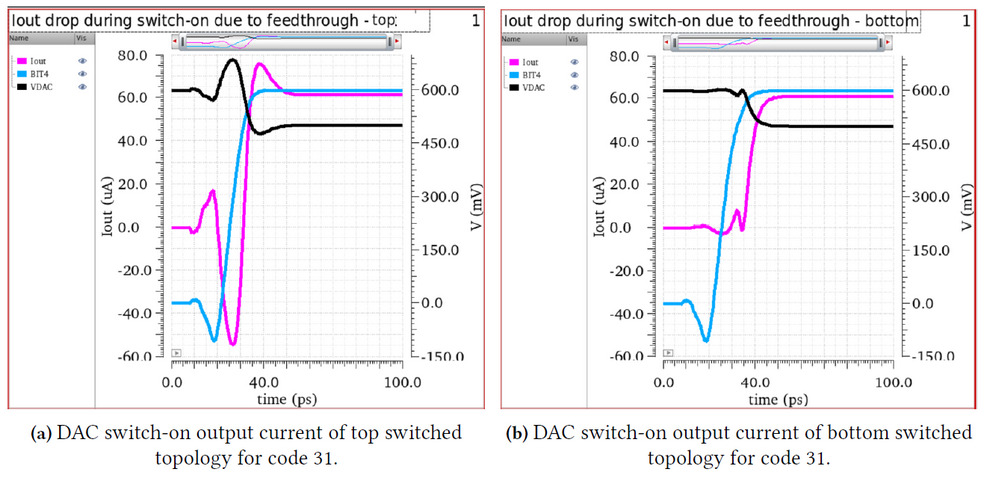
Furthermore the figure shows that the INLEA gets worse when decreasing the averaging time window. This is due to the switching behavior when switching on the current source. These are the purple curves in figure 5. As can be seen here, the bottom switched topology in fig 5b has a less aggressive output current when the current sources are switched on with respect to the top switched topology in fig 5a. One can imagine that when the average window decreases from 100ns to 100ps, the behavior at the start becomes more and more dominant and thus the INLEA increases.
Conclusion
The top switched topology in the DAC has less effect from output current compression and has a better INLEA for averaging time windows larger than 100ps. For DACs that require fast switching output currents, the bottom switched topology will have a better performance. Finally, when looking at the performance of the DAC within the DTC application, the top switched topology is preferred. This is since fast switching of the DAC is not the speed bottleneck of the DTC. This bottleneck is the constant current source which is linearly discharging the capacitor C0.
Figure 4: INLEA of top (left) and bottom (right) switched topologies for different averaging windows. Figure 5: Output current of DAC after switching from code 0 to 31.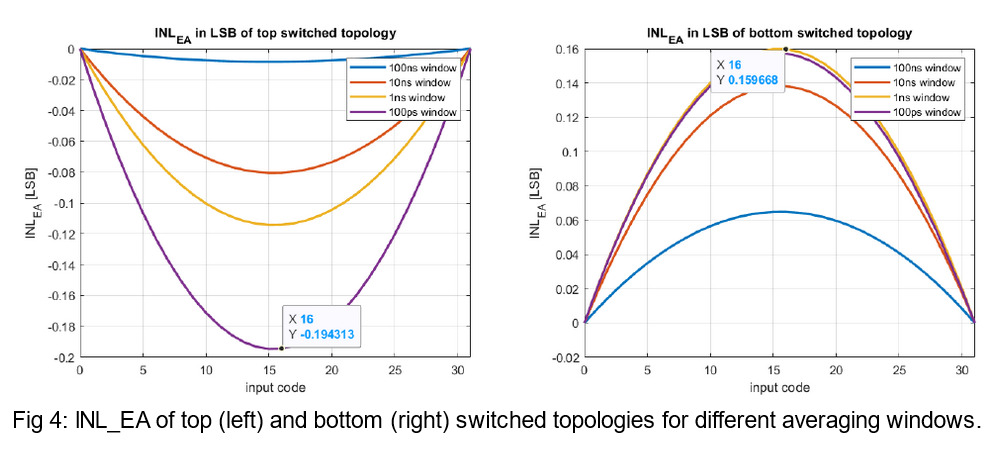
References
[1] J. Z. Ru, C. Palattella, P. Geraedts, E. Klumperink, and B. Nauta, “A High-Linearity Digital-to-Time Converter Technique: Constant-Slope Charging,” IEEE Journal of Solid-State Circuits, vol. 50, no. 6, pp. 1412 – 1423, 2015 , DOI:10.1109/JSSC.2015.2414421