Quantum computers of the future? This material may be the key
You may have seen or read a lot about quantum computers in the past years, like how they have the potential to completely outperform classical computers in terms of computation time for more complex problems. However, the emphasis is on their potential: the main reason we haven’t all thrown our regular computers into the recycling bin and replaced them with quantum computers is that qubits, the quantum equivalent of bits, are extremely unstable. Having functional quantum computers requires exceptionally cold temperatures (not far off from –273.15 °C!), a very isolated system such that the environment does not affect the quantum information, and hence a highly sophisticated error correction protocol. Overcoming the challenges that come with quantum computers are essential as companies such as IBM and Google rapidly develop this novel technology.
Electrical characterization
What if we could create robust qubits that have a high fault-tolerance? This is where topological materials come in with their unique properties: in essence, they allow for encoded quantum information to remain unaffected by local perturbations due to topological states being non-local in nature [2]. In the research that I conducted with the NanoElectronics group at the University of Twente, we investigated tin telluride (SnTe) for its so-called topological crystalline insulating properties. Before this material can be used in any future applications, electrical characterization is essential. The electrical characterization in my paper focused on determining the carrier concentration and mobility in SnTe nanowire devices. My thesis revolved around the design, modeling and measurement of these topological nanowire devices. I will summarize the main findings from my paper in this article and conclude on what is the next step in this research.
Background doping
Before I go further, I want to clarify a few things about the material system. As you may have learned in a course on Semiconductor Physics or similar, materials can principally be insulating, semi-conducting, metallic, or perhaps even semi-metallic. In a nutshell, tin telluride being a topological crystalline insulator means that its bulk is electrically an insulator, while its surface contains conducting states. These metallic surface states are in fact the topological states that we are interested in. However, the real world is of course not so ideal: fabrication of tin telluride involves the generation of many tin vacancies, which act as a massive p-type background doping, masking the topological surface states. So, an important first step in this research is to fabricate tin telluride in such a way that we can suppress this doping as much as possible. Two things have been done in this regard: tin telluride is investigated in the form of nanowires as the surface-to-volume ratio is optimal in increasing the likelihood of observing the surface states of interest during measurements. Something else that is done to decrease the influence of the bulk doping is the alloying of tin telluride with lead telluride, an n-type semiconductor with the same crystal structure. Tuning the tin-lead ratio allows the bulk carrier concentration to be minimized, with one important drawback: at one point, we will lose the topological states that we want to make later use of. You can imagine that optimization during fabrication – which I was not involved in – is not an easy feat, and optimization is still presently going on. Moreover, the nanowires – which are in fact fabricated in Eindhoven – must be made into devices so that measurements can be performed, which can also go wrong and requires multiple iterations to improve the recipe.
Field-effect measurement set-up
Two main measurement set-ups were researched in my paper, one relying on the field-effect, the other on the Hall effect. The field-effect is just as you may know from the field-effect transistor: by applying a gate voltage, we can locally deplete the charge carriers. The carrier concentration is then given by the following formula:
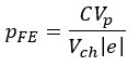
Where C is the capacitance between the nanowire and the gate, V_p is the pinch-off voltage where we have fully depleted the carriers, i.e. the nanowire is insulating, V_ch is the nanowire ’channel’ volume, and e is the elementary charge. In order to determine the nanowire-to-gate capacitance, COMSOL modelling was done, from which we could estimate how many carriers could be depleted for a certain applied gate voltage. At most, carrier concentrations of about 10^19 cm-3 could be depleted in very ideal rectangular nanowires with a diameter of 20 nm for a 10V applied gate voltage. From literature we know that similarly grown SnTe thin-films have concentrations on the order of 2x10^20 cm-3, which implies that it will not be possible to deplete such pure SnTe nanowires without making changes to the material system and/or process flow. Actual measurements were unfortunately not possible as the fabricated devices mostly shorted: this is why the aforementioned optimization of the device fabrication is also critical. Remember, we are dealing with nano-scale devices!
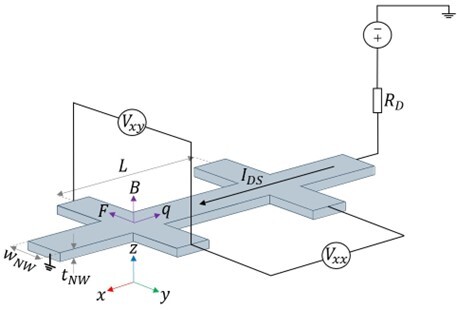
Figure 1: Overview of experimental set-up of a Hall bar device, including relevant geometrical parameters and the Hall effect. The Hall effect results from the Lorentz force on the mobile charges in the nanowire due to the applied magnetic field.
Hall effect measurment set-up
The other measurement method relies on the Hall effect; without going too much into detail, by applying a magnetic field for a small source-drain bias, the charge carriers will deflect from their path and accumulate at the sides of the nanowire. By making use of a Hall bar geometry (see Figure 1), we can determine both the carrier concentration and carrier mobility: the transverse voltage V_xy relates linearly to the magnetic field, and the longitudinal voltage V_xx is theoretically independent of the magnetic field. From these voltages, we can extract the electrical properties of interest. Figure 2 shows the results of these measurements for one nanowire device. The measurement of the transverse ‘Hall’ resistance shows the linear dependence on the magnetic field which we expect, however, the longitudinal resistance shows a dip at zero magnetic field. This dip corresponds to a quantum interference effect known as ‘weak anti-localization’ and it is a first sign of the topological surface states that are of interest to us!
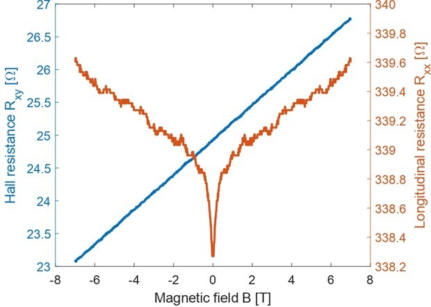
Figure 2: Plot of the transverse and longitudinal resistances versus the magnetic field.
Outcomes of the thesis
Taking all of this into account, during my thesis, it was sadly only possible for me to measure three of our nanowire devices using the Hall effect. All the nanowires were pure tin telluride so that we could not investigate the effect of the tin-lead ratio on the electronic concentrations in our nanowires. So, though I wanted to measure many more nanowires with different ratios and using the two different measurement methods, I realized by the end of my project that while it is good to be optimistic, it will most likely not go as planned, even having anticipated the delays that may occur during my project. But that made it all the more fun, and I still found great results! The data from the COMSOL models give valuable information on the gateability of the transistor devices, and the Hall effect measurements not only gave us a ballpark for the carrier concentrations of pure tin telluride nanowires, but we also saw some first signatures of the topological surface states! For those that are interested, please feel free to take a look at my full paper, where I go into much more detail regarding the experimental set-up and COMSOL model, as well as the assumptions and approximations that I made.
References
1] Adapted from Roche. “Calculating the Unimaginable”. https://www.roche.com/stories/quantum-computers-calculating-the-unimaginable
[2] A. Stern and N. H. Lindner, “Topological Quantum Computation–From Basic Concepts to First Experiments,” Science, vol. 339, no. 6124, pp. 1179–1184, 2013.
Cover picture retreived from: https://www.microsoft.com/en-us/research/blog/microsoft-has-demonstrated-the-underlying-physics-required-to-create-a-new-kind-of-qubit/?lang=fr_ca