Lab-on-a-Chip applications at Benchmark Almelo
A couple of years ago an article was published on how the design team at Benchmark operates, describing our 7-step development model used for our products and the various application fields we are working on. You can find it here: https://vonk.scintilla.utwente.nl/post/2021/benchmark/. In this article we will describe two applications on which this process has been applied, both in the field of Lab-on-a-Chip.
Microfluidic cartridge testing platform
Lab-on-a-Chip (LOC) is a large and growing market. Leveraging small samples of fluid on microfluidic chips for several promising applications, such as clinical diagnostics and personalized drug treatment.
The conversion from micro to macro scale, the connection from the microfluidic device to the analyzing device, poses a few conflicting challenges. To conduct tests, the fluid, gas, and electrical connections must be formed and maintained between the chip and the device. Currently, there are no standards for any of these connections, resulting in many different solutions that have varying shapes and dimensions.
Benchmark Almelo is developing a foundational microfluidic cartridge testing platform to support many microfluidics applications. The platform facilitates multiple fluidic, gas and electric connections between the chip and the device. This platform makes the analysis tools simpler, faster, and cheaper for developers or end users.
Cartridge Architecture
The primary purpose of the cartridge is to house any thickness chips, align them and place their inlet and outlets concentric with the hole pattern integrated in the top of the cartridge. When positioned, the cartridge acts as a bridge between the chip and the machine interface, positioning and aligning the connectors with the corresponding ports or connectors. The four main components of the cartridge are shown in Figure 1. A side view of the assembled cartridge is shown in Figure 2.
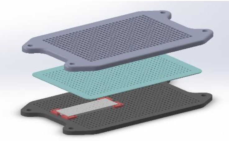
Figure 1: The four main components of the cartridge: top (light grey), seal gasket (green), corner pieces (red), microfluidic chip (white) and bottom (dark grey)
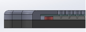
Figure 2: side-view of the cartridge
Connector Architecture and Electrical Interface
The connector between the cartridge and device is a vital aspect of overall design. A good connector design should be user-friendly with a simple closing mechanism that intuitively suggests the closing action. The design should be cost-efficient to manufacture but maintain structural integrity through repeated use.
The platform’s connector plate acts as a backbone for assembling the connectors, simplifying development and prototyping. An engineer can prepare the connector plate on their benchtop and be confident that the connectors will be in the correct position. The fluid connectors are pulled through from the underside until they snap in place.
The electrical connectors are mounted on a pre-made printed circuit board assembly (PCBA), as shown in Figure 3. The pogo pins stick out under the fluid connector flange so they make contact first, pushing the pin in 2mm before the fluid flange mates with the cartridge seal gasket.
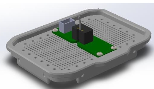
Figure 3: The electrical connectors mounted on a printed circuit board assembly (PCBA)
The assembly with the cartridge placed against the connector plate is shown in Figure 4. The electrical connector diameter is 1mm, which is smaller than the gasket holes. This way, they can reach the chips’ surface, making contact with the electrical pads.
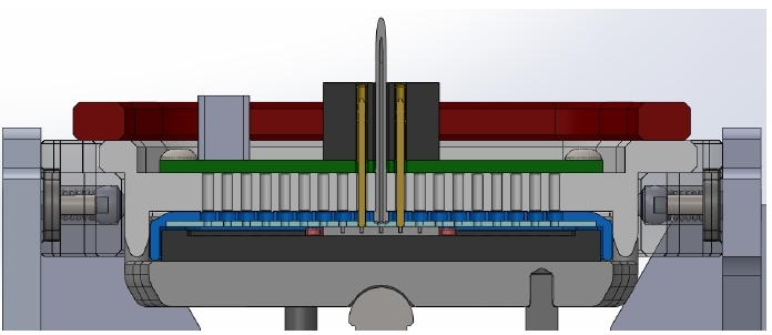
Figure 4: The cartridge placed against the connector plate.
Electrowetting-on-Dielectric
Moving, mixing, and dividing fluidic droplets is a key functionality in many Lab-on-a-Chip applications, such as investigating how certain medication affects a blood or tissue sample or add reactants to ease analysis such as impedance, capacitance or optical measurements. Using droplet manipulation technologies such as electrowetting can greatly decrease the volume needed of these fluids, leading to both a cost decrease for the lab and a benefit for the patient since less fluid needs to be extracted. These technologies also make new applications possible, such as automatic testing of reactions with many varieties of substances where in the past manual steps such as pipetting were needed for each substance used for testing.
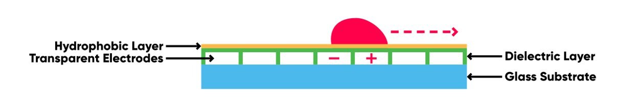
Figure 5: Conceptual overview of electrowetting-on-dielectric
This technique works by using a hydrophobic coating to repel water molecules, causing them to form droplets (see Figure 5). These droplets can then be moved by using electrodes, biased on a relatively high voltage (up to 300V). The droplets will be attracted or repulsed by the electrodes, and since they are oriented in a grid-like fashion and excitable on an individual basis, the droplets can be moved individually, also allowing them to merge (by moving two droplets to the same electrode), mix (by moving the merged droplets around) and split (by attracting two halves of a droplet to opposite directions). See Figure 6 for an example of such an array, with multiple droplets present, differing in size, colour, and position.
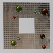
Figure 6: Grid of electrodes with fluid droplets
Realization
The goal of this project was to create an electrowetting board for demonstration and research purposes. After considering multiple alternatives, an architecture for the electrical design was set up, see Figure 7. By using an off-the-shelf computer to control the voltage on the electrodes, the development time of the board was greatly reduced. Furthermore, the high voltage and low voltage parts are separated to ease the I/O between the electrodes and controller.
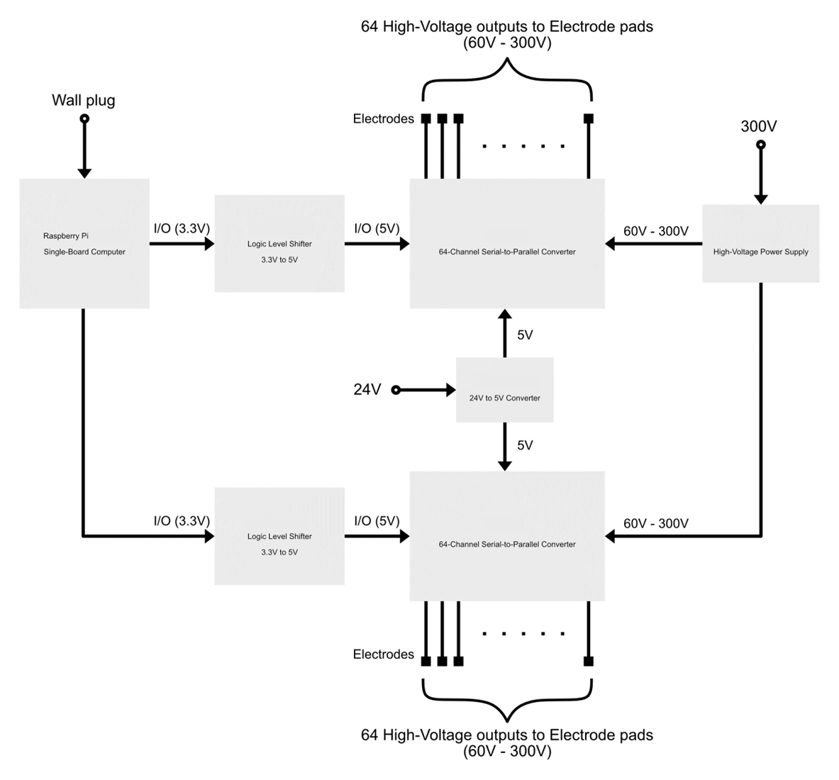
Figure 7: System block diagram
The electrodes can have various shapes, each with their benefits and drawbacks. To investigate the applications and characteristics of each shape, a pattern was developed as shown in Figure 8. The reservoirs can be used to pipette larger amounts of fluid on, after which the other electrodes can be used for the application. The stripped paths can be used to split or merge droplets.
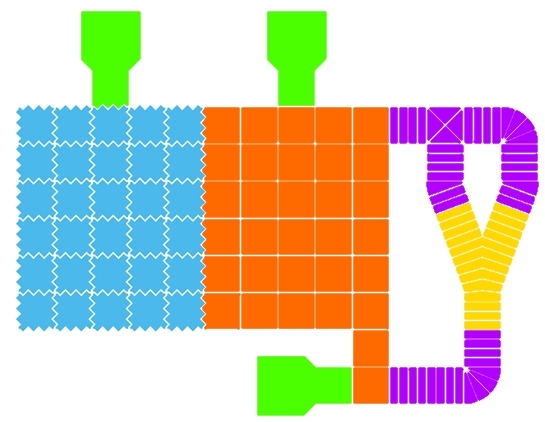
Figure 8: Electrowetting electrode pattern (blue: zig-zag electrodes, orange: square electrodes, purple: strip electrode paths, yellow: Y-splitter, green: reservoirs)
This design has been implemented on a printed circuit board (PCB), see Figure 9. Testing showed that this setup can indeed be used to experiment on electrowetting. The initial design contained solder mask on all the electrodes. During the project it became apparent that removing the solder mask improved the performance of the electrowetting greatly.
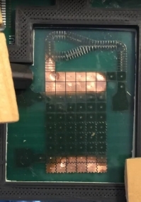
Figure 9: PCB with electrodes
While this is a great start, it is still far from a finished end-product. Recommendations for further research are improving the reliability of the setup, by implementing a feedback system and implementing a controlled dielectric. Furthermore, miniaturization is needed to actually use this in a Lab-on-a-Chip application.
Want to know more?
Are you interested in knowing more about Benchmark, or are you excited to join us for an internship or a job? Visit our website www.werkenbijbenchmark.nl and reach out to us!