How thermal annealing can play a role in reversing degradation in solid-state devices
We live in a digital age in which more and more data is being stored every day. One popular way to store data digitally is through ‘solid-state devices’ such as SSDs, USB drives and SD cards. These devices have an advantage over traditional hard disk drives in that they have higher read and write capabilities.
However as these devices get smaller and smaller to store more data, they come with a downside; they become less reliable over time as their size decreases. During my bachelor assignment I investigated how these solid-state devices degrade over time, and how this degradation can be characterised over time.
![Figure 1: Flash cell structure. Degradation occurs between the floating gate structure and the p-type substrate. $[1]$](keizer1.png)
Figure 1: Flash cell structure. Degradation occurs between the floating gate structure and the p-type substrate. $[1]$
To understand how flash cells (one single cell of flash memory) degrade, it is useful to look at the flash cell structure. Figure 1 shows a low level schematic of a single flash cell. To store data, charge is stored in the floating gate structure by applying a voltage to the word line, allowing charge from the word line to tunnel into the floating gate structure through a process known as Fowler-Nordheim tunnelling. Storing a charge on the floating gate structure also applies an electric field on the NPN structure below, affecting the threshold voltage of the transistor. If the charge increases on the floating gate structure, the threshold voltage increases to a value $V_{T2} > V_{T1}$, where $V_{T1}$ is the threshold voltage if the floating gate structure is uncharged.
To read data stored on a flash cell, a voltage $V_T$ is applied on the word line, which is between $V_{T1}$ and $V_{T2}$. Then a voltage is applied on the bit line, which either allows a current to flow through the NPN structure depending on whether the flash cell is storing charge or not.
Solid-state devices have one drawback however; they are limited in program/erase (PE) cycles due to the mechanisms described above. Every time the floating gate structure is charged and discharged, the oxide layer insulating the floating gate structure becomes electrically stressed. In other words, defects and charge imperfections begin to form in the oxide layer. If enough of these defects form, a phenomenon known as stress-induced leakage current (SILC) can be observed. SILC is bad news for solid-state devices such as SSDs, USB drives and SD cards because it limits the lifetimes of these devices. However, it is also known that the defects formed can be removed through the use of (thermal) annealing. What was not yet clear however, is exactly how the annealing process acts over time.
The goal of my bachelor assignment was to investigate SILC and the subsequent annealing process when annealing an electrically stressed chip at different temperatures. In order to study this, I was able to measure the leakage current present in electrically stressed MOS capacitors instead of flash cells themselves. This is because modern flash cells are small enough that it is not possible to measure a meaningful leakage current using traditional measuring techniques.
$k = Ae^{-\frac{E_a}{k_sT}}$
Equation 1: Arrhenius equation
Equation 1 shows the Arrhenius equation, which was used to characterise the rate of reaction of the thermal annealing process. The Arrhenius equation is used in chemistry to quantify and model the temperature dependence of the rate of reaction of a chemical process. Since the rate of annealing observed in the MOS structures is temperature dependent, it makes sense to use this model as a starting point to characterize the annealing process.
Over the course of several weeks, I was able to measure SILC and the subsequent annealing process in MOS capacitors at several temperatures between 110-230 degrees Celsius. Figure 2 shows one of the I-V curves that I measured whilst annealing a stressed MOS capacitor. Here it is also nicely illustrated that SILC is a more prominent issue at lower voltages.
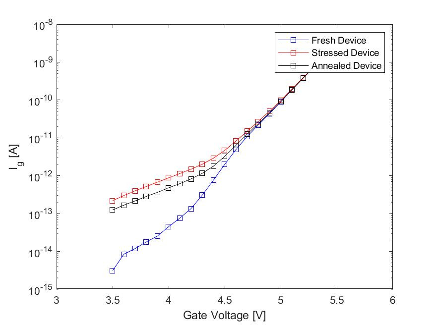
Figure 2: I-V curves showing the mechanism of electrical stressing and thermal annealing at 230 °C.
In conclusion, we can state that the annealing process in MOS capacitors closely follows the Arrhenius equation, whilst showing some second-order temperature dependence. However, extrapolating the measured data for lower temperatures makes annealing at lower temperatures currently unfeasible. Nevertheless, the measurements allows us to get a better understanding of the mechanisms at work behind thermal annealing.
References:
$[1]$ Cyferz, “Flash cell structure,” Wikimedia Commons, July 2007
$[2]$ Wikipedia, “Flash memory” (https://en.wikipedia.org/wiki/Flash_memory)