AnSem’s unique Sizing Tool for analog integrated circuits
Are you biased well to do your job? At AnSem at least our integrated circuits are biased correctly. How come? Because we are using an automated analog IC design process that always results in proper operating modes. We call it the Sizing Tool.
Some of us might know that in the mid 90’s fully automated analog integrated circuit design was a hot topic. Many attempts have been made to create fully automated a transistor circuit based on functional specifications. This turned out to be a step too far. Next, the trend was to make such design software for specific types of circuits only such as amplifiers and opamps. Again, a step too far as this was not efficient, too much preparatory work for too limited return. AnSem was founded in 1998 and followed the automation trend, but starting at capturing the relationships within an analog circuit topology that are easily identifiable. For such, an algorithm can therefore easily do the calculations for you. Does it leave any design freedom and does it require any intellectual effort from the designer? Ironically, you as a designer have to think even harder about the circuit than ever before.
The classical approach is to draw a topology in a schematic entry tool from e.g. Cadence, populate in this schematic the transistor dimensions to your best knowledge, and simulate. After several iterations, having a hard time to keep an overview of all transistor operating points, you will finally come to a proper biased circuit.
What is the AnSem approach? First we draw upon your knowledge to choose the best circuit topology. Please continue studying Electrical Engineering because you will need it. Then you identify for this topology key design choices that can be easily imposed on its devices; what is the absolute current in its output stage, how much noise is allowed in the input stage, how much voltage swing do I want on an intermediate node, should the transistor match with other transistors, etc. After this though mental exercise, that we call engineering, you know from each and every transistor what its job is. Now you can relax and delegate the thinking to … the Sizing Tool. AnSem’s Sizing Tool is a toolbox, written in Matlab that allows to derive for an on-chip electrical device its properties and sizing based on the key design choices and the properties of other devices. You describe your chosen topology and the results of your calculations in predefined functions in Matlab, which is the input for the Sizing Tool. By running the Sizing Tool scripts, all transistors dimensioned will be properly calculated resulting in a guaranteed correct biased circuit. But where is traditional IC design environment? Well, one push button away. A script interprets the Sizing Tool results and will automatically fil in the device properties for the whole schematic. Similar as if you would have done by hand, allowing you to go smoothly to the next step of running simulation for performance verification.
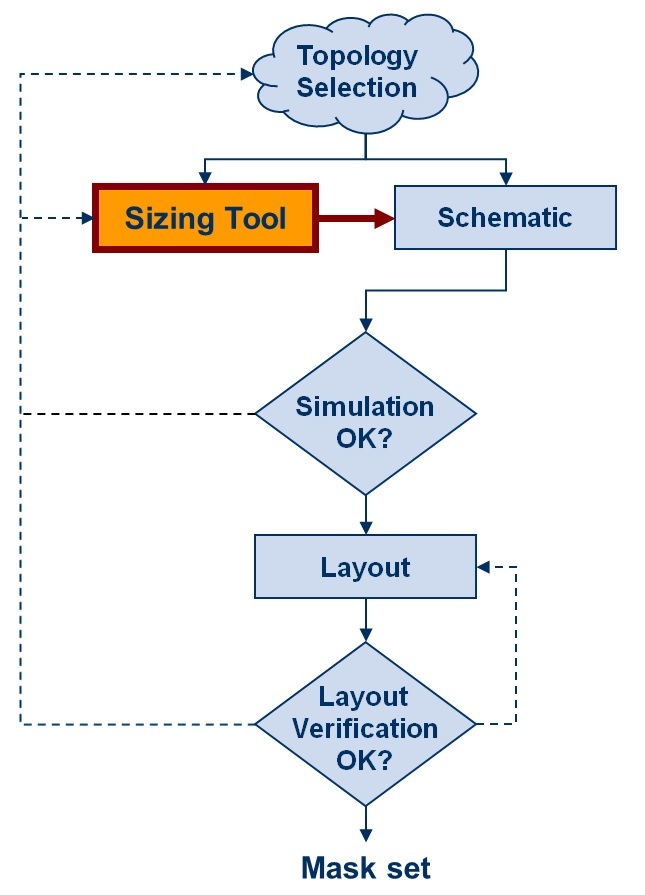
Figure 1: A flowchart of the AnSem Sizing Tool.
This way of design automation has proven to be very useful. The predefined functions, the transistor models derived from the PDK, calculation and control script are AnSem proprietary know-how. We use the Sizing Tool for more the 20 years and are still quite pleased with it. Over these years the Sizing Tool evolved to a mature tool and is very much appreciated by analog circuit designers. In fact, it puts you as designer exactly where you want to be: you do the creative work of engineering and leave the logical resulting calculations up to the tools.